CMOS VLSI

-> Click title to VIEW Circuit
-> Click image to DOWNLOAD Circuit
-> Requires LTSpice

1. CMOS INVERTER

A PMOS NMOS Y
0 on off 1
1 off on 0

combination of pmos and nmos

2. CMOS NAND

parallel PMOS - pull-up network
series NMOS - pull-down network
y = (A.B)'

3. CMOS NOR

output is high when both inputs are low
y = (A + B)'

4. THREE INPUT NOR

NOR is a logic in which output will be high if all 3 input = 0

5. y = ((A.B) + (C.D))' IMPLEMENTATION

in pull-down NMOS network, AND means series, so A.B series
in pull-down NMOS network, AND means series, so C.D series
in pull-up PMOS network, interchange parallel and series for pull-down network

6. y = ((A+B+C).D)' IMPLEMENTATION

In pull-down network,
AND --> Series
OR --> Parallel

In pull-up network,
opposite of pull-down network

7. PASS TRANSISTOR

NMOS pass transistor can pull down to a negative rail but can pull up to a threshold voltage below positive rail
PMOS pass transistor can pull up to a positive rail but can pull down to a threshold voltage above negative rail

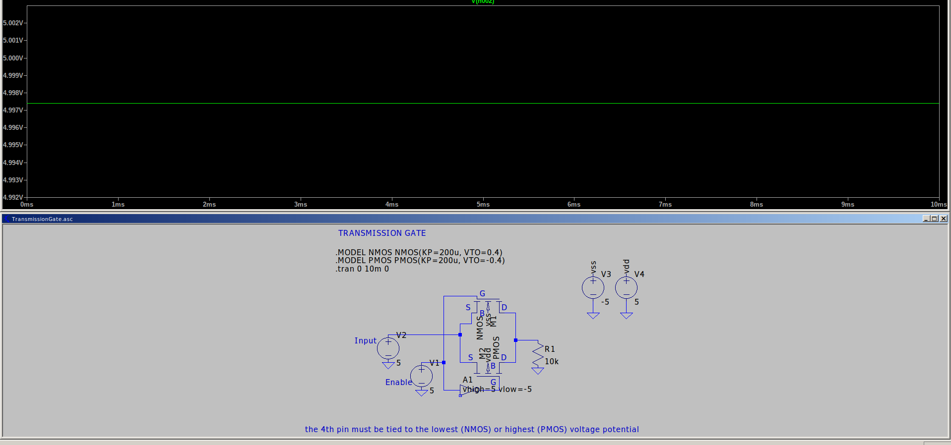
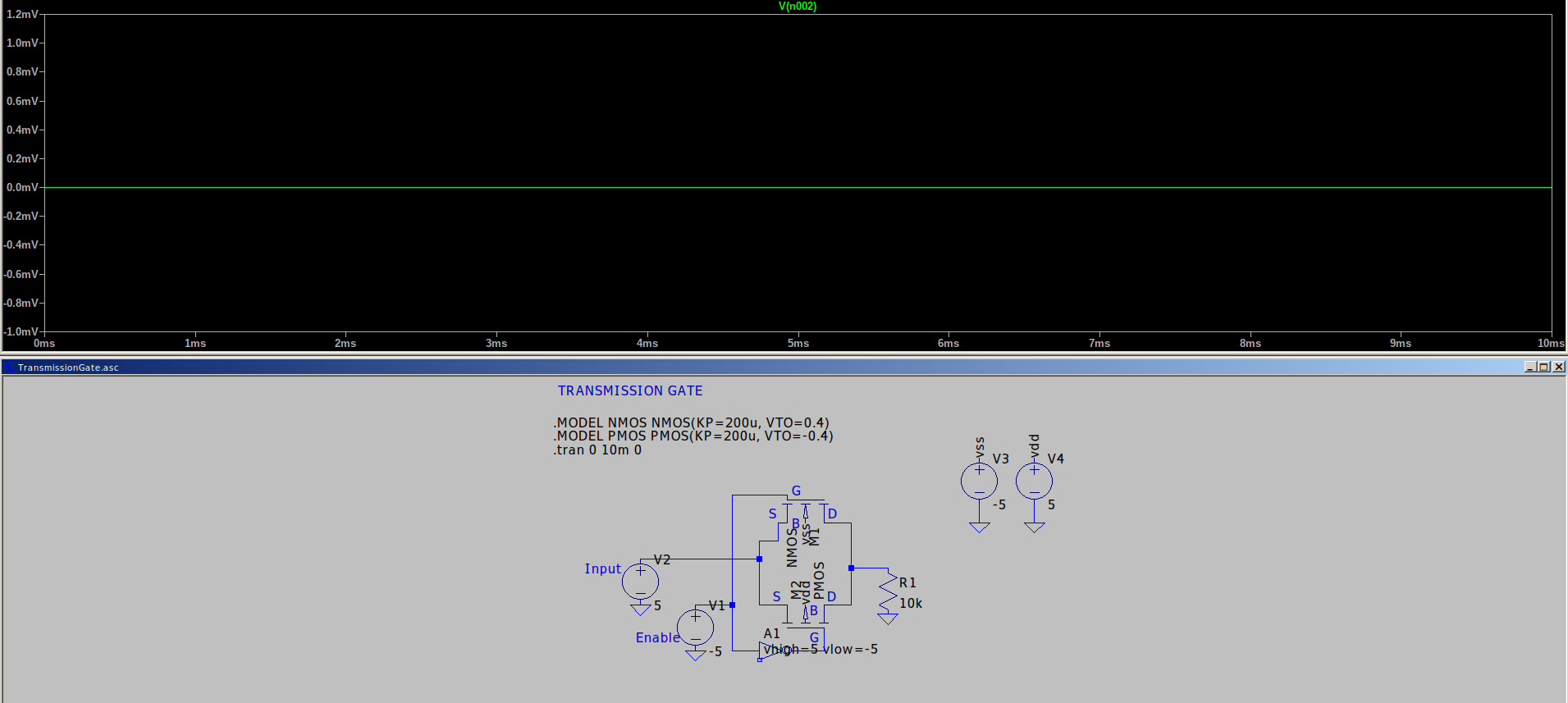
8. TransmissionGate

the 4th pin must be tied to the lowest (NMOS) or highest (PMOS) voltage potential

9. cmos inverter layout

images
spice_works
inverter_magic.spice
inverter_magic.magc
inverter_magic.ext
magic_ngspice_tut.txt

1. CMOS INVERTER Circuit Download
2. CMOS NAND Circuit Download
3. CMOS NOR Circuit Download
4. THREE INPUT NOR Circuit Download
5. y = ((A.B) + (C.D))' IMPLEMENTATION Circuit Download
6. y = ((A+B+C).D)' IMPLEMENTATION Circuit Download
7. PASS TRANSISTOR Circuit Download
8. TransmissionGate Circuit Download
9. cmos inverter layout Circuit Download


hdrohithd 3 years, 3 months ago

How any gates are made into level trigged or edge triggered?
​​​On which basis the construction is different?
​​​​​

hdrohithd 3 years, 3 months ago

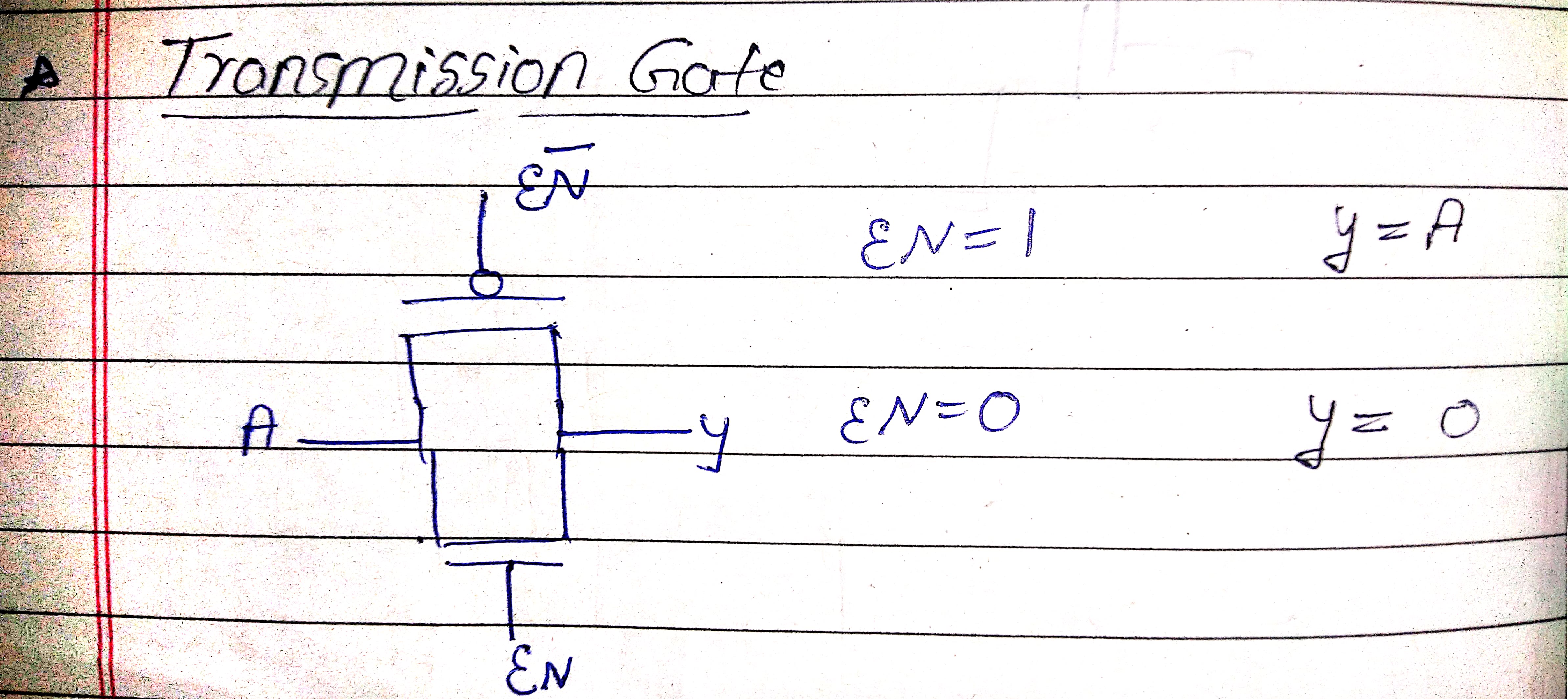
Actually I thought of designing Transmission Gate like this,
but for the drain and source, it's input and output we are providing here, but in nmos source has to be grounded right?

Transmission gate

hdrohithd 3 years, 3 months ago

Yes, I got it, Actually, in the transmission gate, the 4th pin (base pin) must be tied to the lowest (NMOS) or highest (PMOS) voltage potential.
Then it works as expected.


Please login to post comment


🙃 Released on 10/10/2021 as a special of "1 day delayed wish to Father's Birthday, Happy Birthday Appaji..🙃"

Last Updated on Nov. 3, 2021, 3:43 p.m.